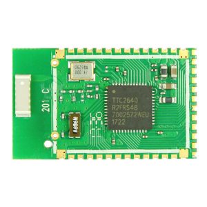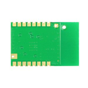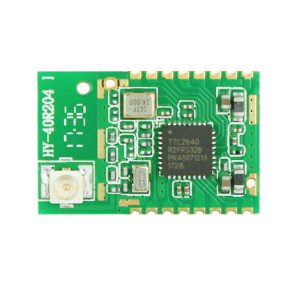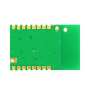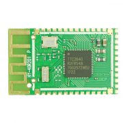
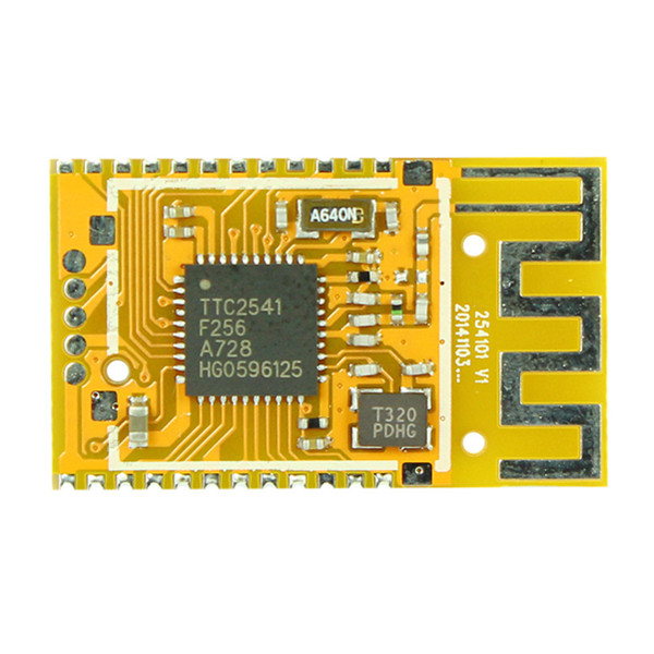
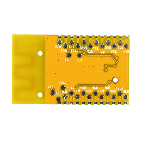
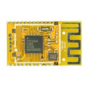
TI CC2541 Bluetooth low energy module WJ-M101
Chipset: TI CC2541
Transmit distance: 30m
Dimension: 15.2*25.3*2.0 mm
- Description
- Inquiry
WJ-M101 BT low energy single mode module is a single mode device targeted for low power sensors and accessories.
It offers all BT low energy features: radio, stack, profiles and application space for customer applications. The module also provides flexible hardware interfaces to connect sensors.
It can be powered directly with a standard 3V coin cell batteries or pair of AAA batteries. in lowest power shutdown mode it consumes only 0.5 uA and will wake up in few microseconds.
It’s transmission distance of 30 meter. (At face to face, free space, 1.2 Meter high from Ground for testing).
Applications:
Heart rate sensors
Pedometers
Watches
Blood pressure and glucose meters
Weight scales
Key fobs
Households sensors and collector devices
Security tags
Wireless keys (keyless go)
Proximity sensors
HID keyboards and mice
Indoor GPS broadcasting devices
KEY FEATURES:
BLE v.4.0 single mode compliant
Supports master,slaveand master/slave modes
Integrated BT low energy stack
GAP, GATT, L2CAP, SMP BT low energy profiles
Compliance: BQB BLE4.0, FCC, IC(Canada), CE ETSI RED…etc. worldwide RF Regulations.
Transmit power :+0dBm typical
Receiver sensitivity: -94dBm typical
In-System-Programmable Flash 256KB SRAM 8KB
Low current consumption :Shutdown. No clocks running, no retention: 0.5uA(Typical)
Wireless Features:
| Bluetooth version | Bluetooth 4.2, support Bluetooth 5.0 |
| Frequency range | 2402-2480MHZ(2.4G ISM) |
| Modulation mode | GFSK |
| Transmit power | -23 – 0dBm |
| Receiving sensitivity | -94dBm(typical) |
| Transparent transmission mode (factory setting required) | Single-connected slave, single-connected host, universal host, beacon, beacon+slave |
| Upgrade method | Support OAD upgrade / support SBL upgrade |
| Transmission distance | 30m(0dBm) |
Hardware Specifications:
| Module size | 25.3*15.2*2.04mm |
| Chipset | CC2541 |
| Module communication interface | UART/SPI/IIC |
| Module pin number | 24PIN |
| Antenna | PCB antenna |
| Working Voltage (DC) | 2.0 – 3.6V |
| Working Temperature | -30℃-+80℃ |
| Storage Temperature | -40℃-+100℃ |
Software Specifications:
| Single link feature | Only supported by 1 host link, can support large packet transmission |
| Single link rate | 1K/S (up to 128 Bytes in a single package, two-way 20ms transmission interval) |
| Baud rate | 9600bps-230400 bps(Default 9600 bps) |
| Parameter configuration | AT command |
| Wireless security | AES |
Power consumption specifications:
| Active-Mode RX | 20.2mA max |
| Active-Mode TX @ 0dBm | 18.2mA max |
| Active-Mode TX @ +5dBm | 9.1 mA max |
| Sleeping mode | 0.45uA avg |
| data transmission | 8.36mA avg |
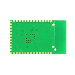
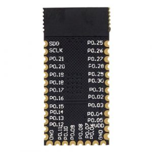
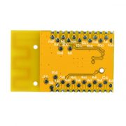
Pin definition and description
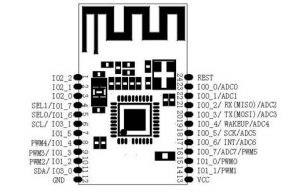
| Pin No. |
Function | Function Description |
| 1 | IO2_2 / DC | Digital I/O port 2_2 / Debug clock |
| 2 | IO2_1 / DD | Digital I/O port 2_1 / Debug data |
| 3 | IO2_0 | Digital I/O port 2_0 |
| 4 | IO1_7 / SEL1 | Digital I/O port 1_7 MCU communication mode select, See table(5-3) Communication protcol mode selection, I/O setting Table |
| 5 | IO1_6 / SEL0 | Digital I/O port 1_6 MCU communication mode select, See table(5-3) Communication protcol mode selection, I/O setting Table |
| 6 | IO3_1 / I2C SCL |
Digital I/O port 3_1 IIC serial Clock (SCL) can be used as I2C clock pin or digital I/O. Leave floating if not used. If grounded disable pull up |
| 7 | IO1_5 | Digital I/O port 1_5 |
| 8 | IO1_4 / PWM4 | Digital I/O port 1_4 / PWM port 4 |
| 9 | IO1_3 / PWM3 | Digital I/O port 1_3 / PWM port 3 |
| 10 | IO1_2 / PWM2 | Digital I/O port 1_2 / PWM port 2 |
| 11 | IO3_0 / I2C SDA |
Digital I/O port 3_0 I2C serial Data (SDA) Can be used as I2C data pin or digital I/O. Leave floating if not used. If grounded disable pull up |
| 12 | GND | BLE module grounding pin |
| 13 | VCC | BLE module power supply pin, voltage range of 2.0 ~ 3.6V |
| 14 | IO1_1 / PWM1 | Digital I/O port 1_1 20mA drive capability / PWM port 1 |
| 15 | IO1_0 / PWM0 | Digital I/O port 1_0 20mA drive capability / PWM port 0 |
| 16 17 |
IO0_7 | Digital I/O port 0_7 |
| ADC7 | ADC port 7 | |
| PWM5 | PWM port 5 | |
| IO0_6 | Digital I/O port 0_6 | |
| 18 19 |
INT | Interrupt output pin |
| ADC 6 | ADC port 6 | |
| IO0_5 | Digital I/O port 0_5 | |
| SPI SCK | SPI Bus clock signal | |
| ADC 5 | ADC port | |
| IO0_4 | Digital I/O port 0_4 | |
| 20 21 22 |
WAKEUP | BLE wake up pin, Low/ wake up, High / BLE module automatically sleep |
| ADC4 | ADC port 4 | |
| IO0_3 | Digital I/O port 0_3 | |
| UART TX | UART Serial data bus output | |
| SPI MOSI | SPI Master Out , Slave input | |
| ADC3 | ADC port 3 | |
| IO0_2 | Digital I/O port 0_2 | |
| UART RX | UART Serial data bus input | |
| SPI MISO | SPI Master input , Slave output | |
| ADC2 | ADC port 2 | |
| IO0_1 / ADC1 | Digital I/O port 0_1 / ADC PORT 1 | |
| 23 | IO0_0 / ADC0 | Digital I/O port 0_0 / ADC PORT 0 |
| 24 | Reset | BLE hardware reset pin (Low: reset) |
Pin Function Description (The module following collectively “BLE”):
a. UART: serial bus, the default baud rate 9600bps, a single packet transmission
is less than 17 bytes, package transmission intervals greater than 20ms.
b. SPI: SPI bus interface, support for less than 2M / S data transmission rate,
a single packet transmission is less than 17 bytes, package transmission intervals greater
than 20ms.
c. IIC: IIC bus interface, support more than 22K / S, less than 400K / S data
transmission rate, a single packet transmission is less than 8 bytes,
package transmission intervals greater than 20ms.
d. MOSI: Master output, Slave input.
e. MISO: Master input, Slave output.
f. SCK: SPI bus clock signal.
g. SDA: IIC data.
h. SCL: IIC clock.
i. WAKEUP: BLE wake up pin, Low _wake up, High/ BLE module automatically sleep.
j. SEL0 & SEL1: MCU and BLE communication mode selection pin. Specific details,
see “(4-3) communication protocol mode selection, I/O setting table “.
k. RESET: BLE hardware reset pin, Low level reset.
l. VCC: BLE module power supply pin voltage range DC 2.0~3.6V.
m. GND: BLE module ground pin.
Related Products
-
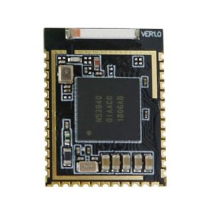
Bluetooth 5.0 TI CC2640 low energy module
Bluetooth 4.2/5.0 low energy module
Chipset: TI CC2640
Size:25.16*15.22*2.0mm
-
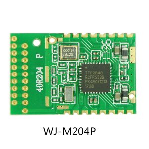
Bluetooth low energy TI CC2541 module
Bluetooth low energy module
Chip set: TI CC2541
Dimension: 15.2*25.3*2.0 mm
-
Ceramic antenna Bluetooth 4.2 low energy module
Ceramic antenna Bluetooth 4.2 low energy module
Chipset: TI CC2640
Size: 11.59*17.9*2.0mm
-
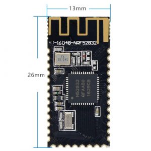
Nordic nrf52832 Bluetooth low energy module
Applications:
Wearable devices
BT intelligent application
Mobile phone accessories
Smart home appliances
Industry control
Data acquisition system -
Bluetooth 4.2/5.0 BLE module
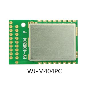
Bluetooth low energy module WJ-M404P/WJ-M404PC
Chipset: TI CC2640
Size:11.59*17.9*2.0mm/11.59*17.9*2.6mm(with shield case)
-
Bluetooth low energy 5.0 nrf52840 module
Applications:
Wearable devices
BT intelligent application
Mobile phone accessories
Smart home appliances
Industry control
Data acquisition system -
External antenna Bluetooth 4.2 low energy module
WJ-M404I Bluetooth low energy single mode module is a single mode device targeted for low energy sensors and accessories.
WJ-M404I offers all Bluetooth low energy features: radio, stack, profiles and application space for customer applications. The module also provides flexible hardware interfaces to connect sensors.
WJ-M404I can be powered directly with a standard 3V coin cell batteries or pair of AAA batteries in lowest power shutdown mode it consumes only 0.15uA and will wake up in few microseconds.
WJ-M404I transmission distance of 100 meter .(At face to face, free space, 1.2 Meter high from Ground for testing).
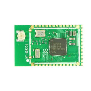
Bluetooth IC:TTC2640R2 4*4*0.9mm 32pin IC,Used TI CC2640R2 die chip -
TI CC2640 Bluetooth BLE module
Bluetooth 5.0 low energy module
Chipset: TI CC2640
Dimension: 25.16*15.22*2.0 mm
-
IPEX connector Bluetooth 5.0 low energy module
Bluetooth 5.0 low energy module
Chipset: TI CC2640
Size:25.16*15.22*2.0mm
-
Bluetooth accelerometer beacon
Bluetooth accelerometer beacon
nRF51822 QFAA chip
CR2032 Battery Holder
Dimension: 26*5mm